Posts

Showing posts with the label Circuit

Flashing LED Battery Status Indicator Circuit

Image
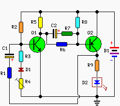
A Battery-status Indicator circuit can be useful, mainly to monitor portable Test-gear instruments and similar devices. LED D1 flashes to attire the user's attention, signaling that the circuit is running, so it will not be left on by mistake. The circuit generates about two LED flashes per second, but the mean current drawing will be about 200µA. Transistors Q1 and Q2 are wired as an uncommon complementary astable multivibrator: both are off 99% of the time, saturating only when the LED illuminates, thus contributing to keep very low current consumption. Circuit operation: The circuit will work with battery supply voltages in the 5 - 12V range and the LED flashing can be stopped at the desired battery voltage (comprised in the 4.8 - 9V value) by adjusting Trimmer R4. This range can be modified by changing R3 and/or R4 value slightly. When the battery voltage approaches the exhausting value, the LED flashing frequency will fall suddenly to alert the user. Obviously, when the batter...

Priject of Receiver and Transmitter Low Cost Data Circuit Diagram

Image
Priject of Receiver and Transmitte r Low Cost Data Circuit Diagram. Here are two simple circuits that can be used for transmission and reception of data via RF to UHF frequency (433MHZ). Two circuits are super simple, no special components and has a good performance, but short range. It is set to the frequency of 433MHZ, but nothing prevents that with some modifications it works on other frequencies.  Receiver and Transmitter Low Cost Data Circuit Diagram 1 The range is small, ideal for data transmissions within an environment like office, garage, laboratory, workshop or room. This system of data communications short-range 434MHz can be used in projects of alarms, electronic gates, trigger devices from a distance, Arduino, etc. .. X1 is working on a crystal harmonic (433.92Mhz) and L1 receiver comprises 1.5 turns of wire must be tested diameter and thickness to reach the perfect reception of the transmitter.  Receiver and Transmitter Low Cost Data Circuit Diagram 2 You can mou...

8 Watt Audio Power Amplifier Circuit Diagram

Image
This is the 8 Watt Audio Power Amplifier Circuit Diagram. This amp can be used as a simple booster, the heart of a more complicated amplifier or used as a guitar amp. It is very small and portable unit and can be powered through 12V battery. I built the circuit on a Vero Board and had to add extra inductors, capacitors and resistors to prevent oscillation. Circuit diagram: 8 Watt Audio Power Amplifier Circuit Diagram Parts: R1 = 47K R2 = 2.2R/1W R3 = 220R/1W R4 = 2.2R/1W C1 = 100nF-63V C2 = 10uF-25V C3 = 470uF-25V C4 = 2000uF-25V C5 = 100nF-63V IC1 = LM383 SPKR = 4ohm/8W Notes: IC1 must be installed on a heat sink. C1 is for filtering and to prevent oscillation and should not be omitted. The circuit can be built on a Vero Board, universal solder board or PC board, the PC board is preferred. The circuit draws about 880Ma at 12 V. By swapping the values of R2 and R3; you can turn this amplifier into a guitar amp with no preamp required. If you can't find 2000uF, then replace C4 with ...

Simple Inverter Overload Protector Circuit Diagram

Image
Simple Inverter Overload Protector Circuit Diagram . An overload condition in an inverter may  permanently  damage  the  power transistor array or burn off the transformer. Some of the domestic inverters sold in the market do not feature an overload shutdown facility, while those incorporating this feature come with a price tag.the circuit presented here is an overload detector which shuts down the inverter  in  an  overload  condition.   Inverter Overload Protector With Delayed Auto Rest Circuit Diagram   It  hasthe following desirable features: It shuts down the inverter and also provides  audio-visual  indication  of  the overload condition. after  shutdown,  it  automatically restarts  the  inverter  with  a  delay  of  6 seconds. thus, it saves the user from the inconvenience  caused  due  to  manually resetting the system or runn...

Burglar Alarm With Timed Shutoff Circuit Diagram

Image
This is a Burglar Alarm With Timed Shutoff Circuit Diagram. When SI (sensor) is closed, power is applied to U2, a dual timer. After a time determined by C2, CI is energized after a predetermined time determined by the value of C5, pin 9 of U2 becomes low, switching off the transistor in the optoisolater, cutting anode current of SCR1 and de-energizing Kl. The system is now reset. Notice that (i6x C2) is less than (R7xC$). The ON time is approximately given by:(R7xC5)-(R6xC2) = Ton  Burglar Alarm With Timed Shutoff Circuit Diagram

Basic Principles of the LC resonance circuit

Image
If so far you are still confused how the actual origin of the resonance between the capacitor and the inductor is in progress, then the simple circuit above will answer your confusion. By understanding a simple electrical circuit above hopefully we will be able to understand the working principle of a series of more complicated and complex that uses the relationship as a series inductor and capacitors transmitter and receiver. Note the picture above, when the switch SW1 is pressed and released back then obtained by the same signal as in the picture above signal. Initially when SW1 is connected to the voltage supply, the capacitor will make filling fast. Then when SW1 is released charge on the capacitor will be used by the inductor as the supply voltage. In accordance with the general nature of the inductor that the DC signal will be considered ordinary wire inductor such that current flowing quickly through the inductor and the charge on the capacitor decreases rapidly exhausted. Uniqu...

Muscular Bio Stimulator for Treatment of Cellulite Circuit Diagram

Image
This is a very simple circuit of a bio-stimulator Muscular, which has indications for the treatment of cellulite. He sends little shocks through two electrodes, and should take great care when using the stimulator. The muscle stimulator circuit is based on a 555 timer IC. The transformer must be 220 volts to 12 100 to 150 mA and the circuit is connected in reverse. Muscular Bio-Stimulator for Treatment of Cellulite Circuit Diagram The IC 555 to generate pulses at 80 Hz and 150usec by the output voltage of the muscle stimulator device is about 60 volts to 150 volts, but the output current is very small and there is no danger of electric shock. The potentiometer P1 bio-stimulator sets the amplitude of the output pulses' and must be operated by the "patient", starting with the knob fully counterclockwise, then rotating it slowly clockwise until the LED begins to light up. The functional principles of the bio-stimulator is the same commercial bio-stimulator. Parts List: Linea...

Ceiling Fan Regulator Motor Speed Control Circuit Diagram

Image
This is a simple ceiling fan regulator circuit diagram. It is used to control the speed of a ceiling fan. In the other words it is an AC motor speed controller circuit, as because it's control the speed of a AC motor(Ceiling Fan).  This ceiling fan regulator circuit built with few numbers of parts. The circuit mainly  based on Z0607 TRIAC. This is a low power AC semiconductor device. Generally which is used to controlling speed of low power ac motor speed.  Circuit Diagram of Ceiling Fan Regulator :      In this ceiling fan regulator circuit , R1=500KΩ is a variable resistor that is used to adjust the fan speed. Capacitor C1 2A104J is a Polyester film capacitor. Pin Diagram of  TRIAC(T1)- Z0607:  Fig: Z0607-TRIAC Pin diagram Pin Diagram of Variable Resistor R1: Fig: Pin Diagram of Variable Resistor Parts List Ceiling Fan Motor Speed Controller circuit: T1 = Z0607 -TRIAC D1 = DB3 C312 -DIAC R1 = 500KΩ -Variable Resistor R2 = 37KΩ -Resistor C1 = 2...

Flash Relay Circuit Diagram

Image
Hello! in this post I will show a very small circuit, the relay opens and closes its contacts intermittently, the speed can be changed by changing the value of C1, the output relay can be turned on an LED, working as a wink - wink! The relay coil and the capacitor voltage is in accordance with the circuit power!  See the figure below:

Emergency lighting using white LEDs Circuit Diagram

Image
This  Emergency lighting using white LEDs Circuit Diagram should be assembled only by experienced people and it is advisable to use a protection network, which can be a light bulb in series. For anyone who is thinking of making a system of emergency lighting and simple, this circuit is a cheap and functional output. The circuit is basically composed of a source AC / DC without a transformer, a charger, a system of automatic switching using a diode and a diode switch to change the brightness.  Emergency lighting using white LEDs Circuit Diagram List of Components R1 = 1M, ¼ Watt, 5% R2 = 10K, ¼ Watt, 5% R3 = 10 Ohms 1Watt All resistors are LED = 22 Ohms, ¼ Watt C1 = 205/400V, PPC C2 = 100uF, 25V Z1 = 9 V, 1 WATT T1 = BD 140 All diodes = 1N4007 BATTERY = 6 volts 4 AH LEDS = WHITE, HIGH EFFICIENCY, 5mm

Basically the DAC circuit

Image
Basically the DAC circuit is made to meet the need for the level of influence in the development of digital electronic circuits electronics world. Since the discovery of Silicon and Germanium semiconductor material then quickly there was a revolution in terms of simplicity and accuracy of an electronic circuit. Besides, with the implementation of digital circuits will support at all in terms of data storage and mobility. Lots of data can now be operated with a computer is a data converted from analog signals. For example a voice signal or analog form of video can be played and stored using a computer after analog signals are converted into digital data. Advantages possessed by the digital data than analog signal is a certainty the nature of the data or logic. Digital data only can be divided into two kinds of logic high "1" and logic low "0". Logic 1 represents 5 volts and low logic voltage 0 volts represents. Examples of the advantages of digital signals over anal...

Rear Light After Glow Circuit Diagram

Image
This article is of interest only to readers whose bicycle lights are powered by a dynamo. The laws on bicycle lights in the United Kingdom are stricter than in other countries and a dynamo is, therefore, a rarity in this country. From the point of view of traffic safety it is advisable (in UK obligatory) for cyclists to have the rear lamp of their bicycle to light even when they are at standstill. In principle, it is not very difficult to modify the existing rear light with afterglow: all this needs is a large enough energy reservoir. Since the after-glow is required for short periods of time only, a battery is not required: a large value capacitor, say, 1 F, is quite sufficient. As the circuit diagram shows, in the present circuit, the normal rear light bulb is replaced by two series-connected bright LEDs, D2 and D3. These are clearly visible with a current of only 6 mA (compared with 50 mA of the bulb). The current is set with series resistor R1. The LEDs are shunted by the 1 F cap...

Digital Stopwatch 0 60 sec Circuit Diagram

Image
Now Build a Digital Stopwatch 0-60sec By using the same circuit of the Digital Stopwatch 0-99sec , we can add an AND gate, and transform the 0 – 99sec stopwatch to a 0 – 60sec stopwatch.We must find a way to control the RESET function of the BCD counter, which is responsible for the counting of the seconds. As we studied above, the circuit resets when we have 99 to 100, that is 1001 1001 à 0001 0000 0000. To make a transformation successfully we must force the pulse from 59 to 60 0011 1001 à 0100 0000 on the output of the BCD counter. Digital Stopwatch 0-60 sec Circuit Diagram  By placing the AND gate, with its inputs on the Q1 and Q2 of the BCD counter of the decades, we make sure that when the gate closes, the RST input of the BCD counter will be set to logical “1”, which on its turn, will force the circuit to start over. The transformed circuit appears in picture 2.

Transistor intercom circuit

Image
Here is a simple but effective intercom circuit that is based fully on transistors.The circuit is based on a three stage RC coupled amplifier. When the push button S2 is pressed, the amplifier circuit wired around T1 & T2 becomes an a stable multi vibrator and starts producing the ringing signals. These ringing signals will be amplified by the transistor T3 to drive the speaker. When the push button S2 is released the circuit will behave as an ordinary amplifier and you can talk to the other side through it. To construct a two way intercom, make two identical copies of the circuit given below and connect it according to the given connection diagram. The stand by current consumption of this circuit is around 20mA. Circuit Diagram Connection Diagram  

1 W mini audio amplifier circuit

Image
In this circuit requires only three components , namely IC TDA7052 , and 2 capacitor electrolyte. Actually , only with IC we are able to run this amplifier , but the sound less than the maximum. This amplifier circuit requires a minimum voltage of 3 volts and 15 volts maximum. Was 1 Watt power output with 4 Ohm impedance. See this circuit below : Just IC and 3 components we can make the circuit above.

6V Ultra Bright LED Chaser Circuit Diagram

Image
This is a spectacular but completely useless project. It lights Ultra-Bright LEDs in a sequence and each LED flashes brightly very briefly. The LEDs light-up going around and around since they are mounted in a circle (on a CD), then they pause before chasing again. The very brief flash of each LED (15ms) and the pauses (1 second) reduce the average current so the battery should last a long time.   For user convenience, this project has a stepper speed control and a brightness control. At slower speeds and/or reduced brightness, the battery’s life is extended considerably. At full brightness, the LEDs flash extremely brightly. More than one of this project grouped together occasionally synchronize, lighting the whole room for a moment. Operation At maximum speed, the LEDs don’t appear to flash, instead they appear to move from one lighted one to the next, around and around. They rotate completely for 4 rotations in two seconds, and then turn off for a one second pause then rep...

Complete Tone Control Circuit Diagram Using TDA2030

Image
This is the Project of  Simple IC TDA2030 Complete tone Control Circuit Diagram. This circuit that use IC TDA2030, but this series is equipped with a tone control. Tone controls include Bass, Treble, and Volume. Power amplifier and tone control has been put together in a single PCB. This amplifier is a mono amplifier type, can be modify for guitar amplifiers .  If not coupled amplifier (mic preamp) then you must deactivated potensio treble and bass, why? because if not using a mic preamp and still maintain potensio treble and bass sound input (input) from the guitar will not or the maximum discharge is not tight on the speakers . So you must deactivated a way to decide which directly connected capacitor  with the tone control circuit, and capacitor were connected directly to potensio volume and input jack.   TDA2030 Complete Tone Control Circuit Diagram PCB Layout   TDA2030 Complete Tone Control Circuit Diagram PCB

Simple Line Activated Solid State Switch Project Circuit Diagram

Image
Let me ask this simply, then explain my use case below. This is a Easy Line Activated Solid State Switch Project . Each and every time a phone on the same line or calling numberis taken off-hook, the circuit will be activated to control an external electronic circuit. If several extension telephones are used on one phone line, the circuit can be useful as a busy indicator. LEDl contains a special flashing red LED that makes an excellent indicator for a busy circuit condition.   Line Activated Solid State Switch Project Circuit Diagram The solid-state switch can be used for several other phone-activated applications, such as automatically turning on a cassette recorder, starting a phone-use timer or counter, etc. A small relay can be connected at points A and B, in place of LEDl, to control external circuits. A 117-Vac-to-6-Vdc plug-in power supply can be substituted for the battery to keep the operating cost at a minimum.  The 48-Vdc, on-hook, phone-line voltage keeps Ql...

Horn Bugle Electronic Circuit Diagram

Image
This Simple Horn Bugle Electronic Circuit Diagram just a door trigger input 4093, bound in a low frequency oscillator, as the transistor Q1, which is the IRF511 FET amplifier is directly connected to a small speaker with horn. The output frequency can be changed by adjusting potentiometer R1. Simple Horn Bugle Electronic Circuit Diagram

Simple Audio Operated Switch Circuit Diagram

Image
This is a simple Audio or voice Operated Switch Circuit Diagram. The sound picked up by SPKRl, which acts as a microphone, is fed to transistor amplifier Ql. The output of Ql is applied across coupling transformer T1 and is used to drive the gate circuit of Triac TRl. TRl is used to lend a latching effect to the action of the relay. Audio Operated Switch Circuit Diagram Sourced By: Circuitsstream