Posts

Showing posts with the label Digital

Digital Stopwatch 0 60 sec Circuit Diagram

Image
Now Build a Digital Stopwatch 0-60sec By using the same circuit of the Digital Stopwatch 0-99sec , we can add an AND gate, and transform the 0 – 99sec stopwatch to a 0 – 60sec stopwatch.We must find a way to control the RESET function of the BCD counter, which is responsible for the counting of the seconds. As we studied above, the circuit resets when we have 99 to 100, that is 1001 1001 à 0001 0000 0000. To make a transformation successfully we must force the pulse from 59 to 60 0011 1001 à 0100 0000 on the output of the BCD counter. Digital Stopwatch 0-60 sec Circuit Diagram  By placing the AND gate, with its inputs on the Q1 and Q2 of the BCD counter of the decades, we make sure that when the gate closes, the RST input of the BCD counter will be set to logical “1”, which on its turn, will force the circuit to start over. The transformed circuit appears in picture 2.

Digital Mains Voltage Indicator

Image
Continuous monitoring of the mains voltage is required in many ap-plications such as manual volt-age stabilisers and motor pumps. An ana-logue voltmeter, though cheap, has many disadvantages as it has moving parts and is sensitive to vibrations. The solidstate voltmeter circuit described here indicates the mains voltage with a resolution that is comparable to that of a general-pur-pose analogue voltmeter. The status of the mains voltage is available in the form of an LED bar graph. Presets VR1 through VR16 are used to set the DC voltages corresponding to the 16 voltage levels over the 50-250V range as marked on LED1 through LED16, respectively, in the figure. The LED bar graph is multiplexed from the bottom to the top with the help of ICs CD4067B (16-channel multiplexer) and CD4029B (counter). The counter clocked by NE555 timer-based astable multivibrator generates 4-bit binary ad-dress for multiplexer-demultiplexer pair of CD4067B and CD4514B.  Digital Mains Voltage Indicator Circ...

SW Converter for Digital AM Car Radio

Image
SW Converter for Digital AM Car Radio Circuit Diagram This circuit is purposely presented with many loose ends (not literally, of course) to stimulate experimenting with RF circuitry at a small outlay. Looking at the circuit diagram you may recognize a modified version of the SW Converter for AM Radios described elsewhere in this issue. The modifications were necessary to make the circuit compatible with a digital rather than analogue AM car radio. The main difference between digital AM radios and their all-analogue predecessors is that tuning is in 9 kHz (some-times 4.5 kHz steps) in compliance with the international frequency allocation for the band. Obviously, that particular step size, desirable as it may be on MW, is a stumbling block if you want to use a digital AM receiver in combination with a frequency step-up converter for SW, where chaos reigns and there is no fixed step size. The first attempt was to make the crystal oscillator variable by about 5 kHz each way.   SW Co...

Digital Clock Date and Thermometer using PIC16F628 PIC16F84 PIC16F690 and DS18S20 or DS18B20

Image
This is a small adjustable clock/date with thermometer function based on PIC16F628 or PIC16F84 microchip and DS18S20 or DS18B20 temperature sensor. The hardware part is very simple because it only uses a pic microcontroller, the DS18S20/DS18B20 sensor, 4x7 segments (common anode, something like KW4-301xxx Series, or common cathode something like CC56-21SURKWA), four transistors, some rezistors! When you first power the device the clock is mentained for 8 seconds. Then the date for 2 seconds and temperature will be displayed for 3 seconds. The clock has four buttons, with one button you enter in set mode, with another button you increase values, the third button will be used to decrease values and you can put or not, the reset. If you don't want a reset button just connect the pin to +5V. You can change: ho -> hour, from 0 to 23 nn -> minutes, from 0 to 59 (I could not display m so I used n twice for it) dd -> date day, from 1 to days/month -> calculated based on month...

Philips 40PFL4609 – Circuit Diagram – Digital main board

Image
Scheamtic – Digital main board - Philips 40PFL4609 The order of pins shown in this diagram is different from that of actual IC3101. IC3101 is divided into seven and shown as IC3101 (1/7) ~ IC3101 (7/7) in this Digital Main Schematic Diagram Section. TYPE-A TYPE-B The order of pins shown in this diagram is different from that of actual IC3101. IC3101 is divided into four and shown as IC3101 (1/4) ~ IC3101 (4/4) in this Digital Main Schematic Diagram Section CONTROL PANEL CIRCUIT FOR BOTH TYPE See the circuit diagram of the SMPS board and other adjustment details =>> CLICK ON THE SCHEMATICS TO ZOOM IN

Analog to Digital Converter Circuit Diagram

Image
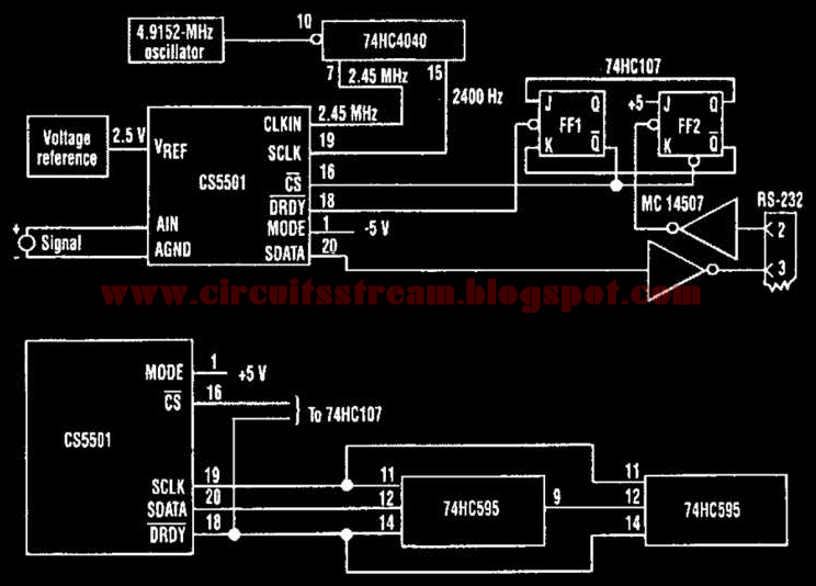
This is a digital Analog to Digital Converter Circuit Diagram. Perhaps the most important consideration of an ADC is its resolution. Because the CS5501 16-bit-delta-sigma analog-to-digital converter lacks a start convert command, it converts continuously, outputting conversion words to its output register every 1024 cycles of its master clock. However, by incorporating a standard dual J-K flip-flop into the circuit, the ADC can be configured to output a single-conversion word only when it is polled.  Analog to Digital Converter Circuit Diagram The CS5501 converter can be operated in its asynchronous communication mode (UART) to transmit one 16-bit conversion word when it is polled over an RS-232 serial line (see figure). A null character (all zeros) is transmitted to the circuit and sets the flip-flop PF2. The CS5501 can then output a single-conversion word, which is transmitted over the RS-232 line as two bytes with start and stop bits. The baud rate can be chosen by selecting t...

Digital Bike Tachometer Circuit Diagram

Image
This is the simple tachometer for bikes uses 2 reed switches to urge the speed data of the bicycle. The reed switches are put in close to the rim of the wheel where permanent magnets pass by. The permanent magnets are connected to the wheelspokes and activate the reed switches everytime they pass by it. The speed is digitally displayed. The tachometer circuit works in step with this principle; the pulses created by the reed contacts are counted inside an explicit time interval. The ensuing count is then displayed and represents the speed of the bike. 2 4026 ICs are used to count the pulses, decode the counter and management 2 7-segment LED show. RS flip-flops U3 and U4 perform as anti-bounce. Electronic bicycle SP tachometer circuit diagram The pulses arrive at the counter’s input through gate U7. The measuring amount is set by monostable multivibrator U5/U6 and might be adjusted through potentiometer P1 so the tacho are often calibrated. The circuit U1/U2 resets the counters. Since ba...

Digital Electronic Lock Circuit Diagram

Image
This Digital Electronic Lock Circuit Diagram shown below uses 4 common logic ICs to allow controlling a relay by entering a 4 digit number on a keypad. The first 4 outputs from the CD4017 decade counter (pins 3,2,4,7) are gated together with 4 digits from a keypad so that as the keys are depressed in the correct order, the counter will advance. As each correct key is pressed, a low level appears at the output of the dual NAND gate producing a high level at the output of the 8 input NAND at pin 13. Digital Electronic Lock Circuit Diagram The momentary high level from pin 13 activates a one shot circuit which applies an approximate 80 millisecond positive going pulse to the clock line (pin 14) of the decade counter which advances it one count on the rising edge. A second monostable, one shot circuit is used to generate an approximate 40 millisecond positive going pulse which is applied to the common point of the keypad so that the appropriate NAND gate will see two logic high levels whe...

Digital tone control with MAX5406

Image
The series will I make here is a series regulator of Volume, Bass, and Balance Trable Digital (Tone Control). The core of this circuit is an IC-type output from the Manufacturer Maxim MAX5406, while the IC is an audio processor that comes with the interface switch hit for Tone Control setting above. The circuit scheme is as follows: The scheme above uses very little supporting components and this makes can be made with a mini size of a matchbox only even if using all SMD components can be reduced in size by half for this time I will only give a simple layout made​​, following picture: layout components

Digital Clock with Timer and Solar Panel Regulator

Image
This is a combination digital clock timer and solar panel charge controller used to maintain a deep cycle battery from a solar panel. The timer output is used to control a 12 volt load for a 32 minute time interval each day. Start time is set using 9 dip switches and ends 32 minutes later. The 32 minute duration is set by selecting the 5th bit (2^5 = 32) of a 4040 binary counter (pin 2). The timer also has a manual toggle switch so the load can be manually switched on or off and automatically shuts off after 32 minutes. The time duration can be longer or shorter (8,16,32,64,128,256 minutes etc.) by selecting the appropriate bit of the counter. The timer circuit is shown in the lower schematic just above the regulator.   Basic Clock Circuit diagram The basic clock circuit (top schematic below) is similar to the binary clock (on another page) and uses 7 ICs to produce the 20 digital bits for 12 hour time, plus AM and PM. A standard watch crystal oscillator (32,768) is used as the tim...

Digital Frequency Comparator Circuit Diagram

Image
Here’s a digital frequency comparator for oscillators that indicates the result through a 7-segment display and a light-emitting diode (LED). When the frequency count of an oscillator is below ‘8,’ the corresponding LED remains turned off. As soon as the count reaches ‘8,’ the LED turns on and the 7-segment display shows ‘8.’ This demo circuit uses two NE555 timers configured as astable free-running oscillators, whose frequencies are to be compared. The circuit of the digital frequency comparator portion comprises two 74LS90 decade counter ICs (IC2 and IC6), two 74LS47 7-segment display driver ICs (IC3 and IC7), 74LS74 set/reset flip-flop (IC4), 74LS00 NAND gate (IC8) and two 7-segment displays (DIS1 and DIS2). The astable free-running oscillators built around the timers are the frequency sources for the corresponding counters. Digital Frequency Comparator Circuit Diagram When power supply to the circuit is switched on, timing capacitor C1 starts charging through resistor R1 and potmet...

Digital Potentiometer Using DS1669

Image
This DS1669 digital potentiometer circuit can be used for replacing your manual volume control in audio circuits.DS1669 are digital rheostats or potentiometers and provide 64 possible uniform tap points over the resistive range and are available in standard versions of 10K, 50K, and 100K ohms.The IC can be controlled by either a mechanical–type contact closure input or a digital source input such as a CPU With this circuit we can control sound volume form an stereo audio amplifier. Digital Potentiometer Circuit Using DS1669 When the S1 and S2 is push we can modify the level of sound (up or down). This integrated circuit is manufactured by Dallas Semiconductor and it can be use like a potentiometer in many applications like : contrast adjustment for an LCD or for level sound control. This digital volume controller IC is manufactured in dip or soic footprint (8 pins) and can be supply with an voltage between 4.5 and 8 volts DC.

Digital Signals and Gates

Image
While the binary numeration system is an interesting mathematical abstraction, we haven’t yet seen its practical application to electronics. This chapter is devoted to just that: practically applying the concept of binary bits to circuits. What makes binary numeration so important to the application of digital electronics is the ease in which bits may be represented in physical terms. Because a binary bit can only have one of two different values, either 0 or 1, any physical medium capable of switching between two saturated states may be used to represent a bit. Consequently, any physical system capable of representing binary bits is able to represent numerical quantities, and potentially has the ability to manipulate those numbers. This is the basic concept underlying digital computing. Electronic circuits are physical systems that lend themselves well to the representation of binary numbers. Transistors, when operated at their bias limits, may be in one of two different states: eith...

Two button Digital Lock

Image
Now here’s a digital lock unlike any other, as  it has only two buttons instead of the usual  numeric keypad. The way it works is as simple  as its keypad. Button S1 is used to enter the  digits of the secret code in a pulsed fashion-i.e. the number of times you press the but-ton is determined by the digit to be entered.  A dial telephone uses the same type of coding (now maybe there’s an idea?). Press four  times for a 4, nine times for a 9, etc. Pressing button S2 indicates the end of a digit.    Project Image :    Two-button Digital Lock Project Image   For example, to enter the code 4105, press  S1 four times, then press S2, then S1 once, S2  once, then without pressing S1 at all, press S2  again, then finally S1 five times and S2 once  to finish. If the code is correct, the green LED D1 lights for 2 seconds and the relay is energised for 2 seconds. If the code is wrong, the  red LED D2 lights for 2 seconds, and the relay  is not energised. To change the code, fit a jumper to...

Digital Clock with MM5314N

Image
Description  The digital clock of circuit, has as base one IC, the MM5314N, in which are contained all the circuits that need. The IC1 collaborates with six Display of common anode, that are not critically as materials. You can select what dimension, you want it is enough you adapt pins their in the circuit. The display are drive by a system of polyplexis and are drive by thirteen transistors. For timing the circuit, is used the frequency of network (50HZ). This solution is the simplest, that it is not best. For more constant frequency you can use a circuit that would be based on crystal, (it will be given shortly). For the clue of hour are used six display of 7 element common anode. The DS1-DS2, show the hours (decades-unit respectively), the DS3-DS4, show the minutes and DS5-DS6, the seconds. The common anode, for each display is drive by the collector of transistors Q8 until Q13. Individual led (a, b, c, d, e, f, g) the display, they are linked between them (parallel) and are dr...

Digital Electronic Lock Circuit Diagram

Image
This Digital Electronic Lock Circuit Diagram shown below uses 4 common logic ICs to allow controlling a relay by entering a 4 digit number on a keypad. The first 4 outputs from the CD4017 decade counter (pins 3,2,4,7) are gated together with 4 digits from a keypad so that as the keys are depressed in the correct order, the counter will advance. As each correct key is pressed, a low level appears at the output of the dual NAND gate producing a high level at the output of the 8 input NAND at pin 13. Read : Cheap Bicycle Alarm Schematics Circuit Digital Electronic Lock Circuit Diagram The momentary high level from pin 13 activates a one shot circuit which applies an approximate 80 millisecond positive going pulse to the clock line (pin 14) of the decade counter which advances it one count on the rising edge. Read : Emergency Light and Alarm Circuit Diagram A second monostable, one shot circuit is used to generate an approximate 40 millisecond positive going pulse which is applied to the ...

Digital Dice With 7 Segment Display

Image
A digital dice circuit can be easily realised using an astable oscillator circuit followed by a counter, display driver and a display. Here we have used a timer NE555 as an astable oscillator with a frequency of about 100 Hz. Decade counter IC CD4026 or CD4033 (which-ever available) can be used as counter-cum-display driver. When using CD4026, pin 14 (cascading output) is to be left unused (open), but in case of CD4033, pin 14 serves as lamp test pin and the same is to be grounded. Circuit diagram :   Digital Dice With 7-Segment Display Circuit diagram The circuit uses only a handful of components. Its power consumption is also quite low because of use of CMOS ICs, and hence it is well suited for battery operation. In this circuit two tactile switches S1 and S2 have been pro-vided. While switch S2 is used for initial resetting of the display to ‘0,’ depression of S1 simulates throwing of the dice by a player. When battery is connected to the circuit, the counter and display secti...