Posts

Showing posts from June, 2017

Motorbike Alarm

Image
This simple to build alarm can be fitted in bikes to protect them from being stolen. The tiny circuit can be hidden anywhere, without any complicated wiring. Virtually, it suits all bikes as long as they have a battery. It doesn't drain out the battery though as the standby current is zero. The hidden switch S1 can be a small push-to-on switch, or a reed switch with magnet, or any other similar simple arrangement. The circuit is designed around a couple of low-voltage MOSFETs configured as monostable timers. Motorbike key S2 is an ignition switch, while switch S3 is a tilt switch. Motorbike key S2 provides power supply to the gate of MOSFET T2, when turned on. When you turn ignition off using key S2, you have approximately 15 seconds to get off the bike; this function is performed by resistor R6 to discharge capacitor C3. Thereafter, if anyone attempts to get on the bike or move it, the alarm sounds for approximately15 seconds and also disconnects the ignition circuit. During parki

zBot 10 A Power Stage for DC Motor Circuit Diagram

Image
zBot :10-A Power Stage for DC Motor Circuit Diagram . If you look at the chassis of the zBot vehicle1, you’ll find two parts requiring intelligent control: the steering servo and the DC motor . The so called H-bridge is the normal circuit for electronic control of revolution speed and direction. The DC motor of a Tamiya car is powerful enough to propel zBot at up to 20 miles per hour. . The motor then consumes more than 10 A, so we choose high-current power MOSFETs for the driver stage. There are lots of different devices to choose from. The MOSFET we require has to supply the maximum motor current and, importantly, it has to be switched with gate voltages of about 5 V. In this case, the microcontroller switches the power stage (‘low side’) directly. For high side driving level shifters are necessary. The schematic of the H-bridge power stage shows a few inverters, NAND gates and two tri-stateable drivers. These logic functions are very important as the easier way, i.e.., directly con

Four Stage FM Transmitter

Image
This FM transmitter circuit uses four radio frequency stages: a VHF oscillator built around transistor BF494 (T1), a preamplifier built around transistor BF200 (T2), a driver built around transistor 2N2219 (T3) and a power amplifier built around transistor 2N3866 (T4). A condenser microphone is connected at the input of the oscillator.  Four-Stage FM Transmitter Circuits diagram : Four-Stage FM Transmitter Circuits Diagram Working of the circuit is simple. When you speak near the microphone, frequency-modulated signals are obtained at the collector of oscillator transistor T1. The FM signals are amplified by the VHF preamplifier and the pre-driver stage. You can also use transistor 2N5109 in place of 2N2219. The preamplifier is a tuned class-A RF amplifier and the driver is a class-C amplifier. Signals are finally fed to the class-C RF power amplifier, which delivers RF power to a 50-ohm horizontal dipole or ground plane antenna. Use a heat-sink with transistor 2N3866 for heat dissip

Pushbutton Relay Selector

Image
This circuit was designed for use in a hifi showroom, where a choice of speakers could be connected to a stereo amplifier for comparative purposes. It could be used for other similar applications where just one of an array of devices needs to be selected at any one time. A bank of mechanically interlocked DPDT pushbutton switches is the simplest way to perform this kind of selection but these switches aren’t readily available nowadays and are quite expensive. This simple circuit performs exactly the same job. It can be configured with any number of outputs between two and nine, simply by adding pushbutton switches and relay driver circuits to the currently unused outputs of IC2 (O5-O9). Gate IC1a is connected as a relax-ation oscillator which runs at about 20kHz. Pulses from the oscillator are fed to IC1b, where they are gated with a control signal from IC1c. The result is inverted by IC1d and fed into the clock input (CP0) of IC2. Initially, we assume that the reset switch (S1) has be

12 Frequently Asked Questions

List of most frequently asked question list is given in below : FAQs by customers Here we are going to discuss following question asked by customers from various fields like cement industries, steel sectors, paper mill etc. Q1) What are the indicators of mechanical life of contactors? Q2)Which application criteria shall be considered for use of contactors on line side of variable speed drives? Q3) Which application criteria shall be considered for use of contactors on load side of variable speed drives? Q4)What are the derating factors for Contactors at higher frequencies ? Q5) How do I calculate the critical length on control cable for contactor? Q6)Is there any guidelines available to determine the correct size of control transformers? Q7)What is Effect of Cable Capacitance on the Operation of AC operated Contactors 8)How to calculate power loss of contactors which is generally required for thermal calculations of a switchboard 9)Which technical consequences shall be considered i

Build a 10 Amp Solar Charge Controller SCC2 Circuit

Image
The SCC2 is a solar charge controller, it’s function is to regulate the power flowing from a photovoltaic panel into a rechargeable battery. It features easy setup with one potentiometer for the float voltage adjustment, an equalize function for periodic overcharging, and automatic temperature compensation for better charging over a range of temperatures. 10 Amp Solar Charge Controller Circuit Diagram With Parts List The goal of the circuit design was to make a charge controller with analog simplicity, high efficiency, and reliability. A medium power solar system can be built with a 12V solar panel up to 10 amps, the SCC2, and a lead acid or other rechargeable up to a few hundred amp hour capacity. The SCC2 can be operated at battery voltages other than 12V, it can work at 6V and 24V by changing a few parts. Operation at voltages between 6V and 24V is also possible. Specifications Maximum solar panel current: 10 Amps Night time battery drain current: approximately 1ma Nominal battery v

Analog to Digital Converter Circuit Diagram

Image
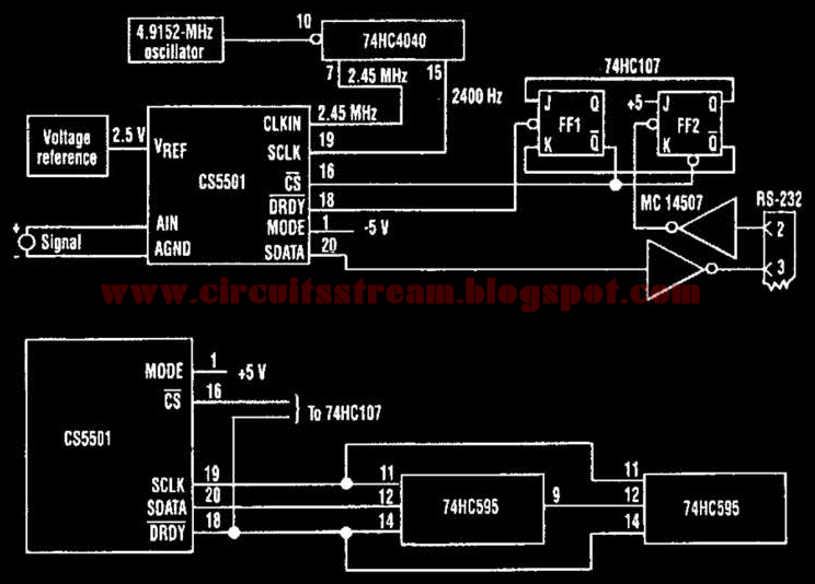
This is a digital Analog to Digital Converter Circuit Diagram. Perhaps the most important consideration of an ADC is its resolution. Because the CS5501 16-bit-delta-sigma analog-to-digital converter lacks a start convert command, it converts continuously, outputting conversion words to its output register every 1024 cycles of its master clock. However, by incorporating a standard dual J-K flip-flop into the circuit, the ADC can be configured to output a single-conversion word only when it is polled.  Analog to Digital Converter Circuit Diagram The CS5501 converter can be operated in its asynchronous communication mode (UART) to transmit one 16-bit conversion word when it is polled over an RS-232 serial line (see figure). A null character (all zeros) is transmitted to the circuit and sets the flip-flop PF2. The CS5501 can then output a single-conversion word, which is transmitted over the RS-232 line as two bytes with start and stop bits. The baud rate can be chosen by selecting the a

Miniature High Rate Speed Control with BEC Project

Image
This is a Miniature High-Rate Speed Control with Battery Eliminator Circuit (BEC) . This design is based on one published by Milan Lulic in the German magazine elektroModell. Mr. Lulic’s design is for surface mount technology (SMT) construction, whereas mine uses standard off-the-shelf components, and is therefore better suited to construction by the hobbyist. The circuit begins with a buffer, consisting of C1, R1, and Q1. This provides some isolation between the receiver and the rest of the circuit, and makes circuit operation somewhat independent of the model of receiver (although you may have to adjust R8 if you change receiver types). R2, R3, and C2 form an integrator, which produces an output voltage proportional to the pulse width of the input signal. This output voltage varies from approximately 1.15V for a 1ms input to 1.45V for a 2ms input (at 50 pulses per second). Z1A, together with R4 through R8, and C3, form a 2.5kHz triangle wave generator. R8 adjusts the upper and lower

Pulse Sequence Detector

Image
It is a very simple electronic Schematic Circuit Diagram of Pulse sequence detector Circuit. The resistor divider connected between Ql and Q2 supplies IH to Ql after input A triggers it.  Pulse Sequence Detector Circuit Diagram: It also prevents input from triggering Q2 until Ql conducts.Consequently, the first input pulse after input A is applied will supply current to RL.

Simple Relay Step Up Circuits

Image
Have you ever needed to power a 12-volt relay in a circuit but only had 6 or 9 volts available? This simple circuit will solve that problem. It allows 12-volt relays to be operated from 6 or 9 volts, or 24-volt relays from 12 volts. While most normal relays require the manufacturer-specified coil voltage to reliably pull the contacts together, once the contacts are together you only need about half that rated voltage to hold them in. This circuit works by using that principle to provide a short burst of twice the supply voltage to move the contacts and then applies the available 6 or 9 volts to the relay to lock the contacts in place. With reference to Figure A., when the main supply is applied to the circuit the 220-µF capacitor, C1, charges quickly to +6 volts through resistor R3. The circuit is now awaiting voltage on the control input. When a control voltage (can be as little as 3 volts) is applied to the control input, transistor T1 switches on. The other transistor, a BC558, is a

Reducing Treble tone circuit

Image
Treble reducer circuit above is an example of a simple circuit and is suitable to be used as experimental material and analysis of the workings of the circuit.  As I mentioned earlier the bass reducer series, this series actually has the same working principles with a series of bass reducer. Where these circuits utilize capacitors nature of the charge and discharge. The difference of the damping function obtained from the difference of the capacitor. If the series bass reducer series capacitors are mounted on the op-amp input lines, while in this treble reducer series capacitors are mounted parallel with the strengthening of the op-amp prisoners. Installation of this circuit has a parallel in the work analysis in contrast with the installation of the series on a series of bass reducer. The difference is that the installation of the series, so we URLs that are easy to understand how a wire working capacitors for high frequency signal, so with high frekuesni so automatic signal to be pas

Battery Equality Monitor Circuit Diagram

Image
Almost all 24V power systems in trucks, 4WDs, RVs, boats, etc, employ two series-connected 12V lead-acid batteries. The charging system can only maintain the sum of the individual battery voltages. If one battery is failing, this circuit will light a LED. Hence impending battery problems can be forecast. The circuit works by detecting a voltage difference between the two series connected 12V batteries. Idle current is low enough to allow the unit to be permanently left across the batteries. Circuit diagram: Battery Equality Monitor Circuit Diagram Parts: R1 = 2.K R2 = 4.7K R3 = 39K R4 = 39K R5 = 1.5K R6 = 1.5K Q1 = BC547 Q2 = BC547 Q3 = BC557 D1 = 3mm Red LED D2 = 3mm GreenLED B1 = DC 12 Volt B2 = DC 12 Volt

Simple Doorbell for the Deaf

Image
This electronic circuit provides a delayed visual indication when a door bell switch is pressed. In addition, a DPDT switch can be moved from within the house which will light a lamp in the door bell switch. The lamp can illuminate the words "Please Wait" for anyone with walking difficulties. Simple Doorbell for the Deaf Circuit Diagram: Notes The circuit uses standard 2 wire doorbell cable or loudspeaker wire. In parallel with the doorbell switch, S1, is a 1N4001 diode and a 12 volt 60mA bulb. The bulb is optional, it may be useful for anyone who is slow to answer the door, all you need to do is flick a switch inside the house, and the bulb will illuminate a label saying Please Wait inside the doorbell switch or close to it. The double pole double throw switch sends the doorbell supply to the lamp, the 22 ohm resistor is there to reduce current flow, should the doorbell switch, S1 be pressed while the lamp is on. The resistor needs to be rated 10 watts, the 0.5 Amp fuse prot

TSM May be Sole Manufacturer of AAPL A8 Chips for iPhone 6

Image
Taiwan Semi (TSM) May be Sole Manufacturer of Apple's (AAPL) A8 Chips for iPhone 6. Taiwan Semi (NYSE: TSM) is up in early trading Wednesday following reports that the company might have scored a big chip deal. Taiwam's Commercial Times reported that Taiwan Semi was tapped to supply the A8 chip in Apple's upcoming iPhone 6. The news is positive for Taiwan Semi and also hints that Apple is further distancing itself from rival Samsung. Production on the chips, which use a 20-nanometer process and have a 64-bit processor core, was said to begin in February. Taiwan Semi was also said to get most of the manufacturing orders for logic and power management integrated chips (ICs). Jefferies said earlier Wednesday that the iPhone 6 might debut in late summer and the Commercial Times is also looking for a Q314 launch. Finally, the Commercial Times thinks revenue for Q214 will rise 20 to 25 percent, better than previous market forecasts calling for a 15 to 20 percent gain. Taiwan Semi

Simple Reset Protection For Computers Circuit Diagram

Image
This is the simple Reset Protection For Computers Circuit Diagram. This protection circuit is inserted between the reset switch and the motherboard. The earth connection of the computer must be linked to terminal of the protection circuit. The protection circuit can draw its power from the computer supply. When the circuit has been fitted, operation of the reset switch will not immediately restart the computer. Instead, a buzzer will sound to alert you to the reset operation.    Simple Reset Protection For Computers Circuit Diagram The buzzer is actuated for 4 s by monostable IC1A, which is triggered by the reset switch. During these 4 s, the output, pin 5, of IC1A ensures that the reset function, pin 10, of IC1B is disabled. When the reset switch is operated again, monostable IC IB will be triggered and this starts the reset procedure. Transistor T2 is then switched on for 0.5 s and the buzzer is deactuated via Rll and D4. The circuit around T1 and N4 ensures that IC1A can accept trig

Simple Car Alarm Arming Horn Beep Canceller Project

Image
This is the Simple Car Alarm Arming Horn Beep Canceller Circuit Diagram Project. It's a great convenience that most modern cars come with a built in alarm, however it is nothing but noise pollution that the horn sounds when the alarm is armed. Disconnecting the alarm system from the horn relay will eliminate this, but prevent the horn from sounding in the even of an actual alarm. This circuit serves to silence the arming beep yet maintain the alarm by introducing a small delay into the signal.    Car Alarm Arming Horn Beep Canceller Circuit Diagram       It sits between the alarm and horn relay. The alarm must provide a constant horn signal for at least 3 seconds before the horn relay is activated. That way the quick "beep" will never activate the horn relay, while the constant alarm signal will. Part           Total Qty.             Description C1                   1           0.01uF Ceramic Disc Capacitor   C2                   1           100uF 35V Electrolytic Capacit

Electronical 6V to 12V Converter Circuit Diagram

Image
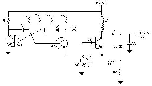
      This is the Simple Electronically 6V to 12V Converter Circuit Diagram. This inverter circuit can provide up to 800mA of 12V power from a 6V supply. For example, you could run 12V car accessories in a 6V (British?) car. The circuit is simple, about 75% efficient and quite useful. By changing just a few components, you can also modify it for different voltages.  Electronical 6V to 12V Converter Circuit Diagram Parts R1, R4           2    2.2K 1/4W Resistor    R2, R3           2    4.7K 1/4W Resistor    R5    1            1K 1/4W Resistor    R6    1            1.5K 1/4W Resistor    R7    1            33K 1/4W Resistor    R8    1            10K 1/4W Resistor    C1,C2            2    0.1uF Ceramic Disc Capacitor    C3    1            470uF 25V Electrolytic Capcitor    D1    1            1N914 Diode    D2    1            1N4004 Diode    D3    1             2V 400mW Zener Diode    Q1, Q2, Q4    3    BC547 NPN Transistor    Q3    1           BD679 NPN Transistor    L1    1           See

2 Watt Audio Amplifier Circuit Diagram

Image
This amplifier was designed to be self-contained in a small loudspeaker box. It can be feed by Walkman, Mini-Disc, iPod and CD players, computers and similar devices fitted with line or headphone output. Of course, in most cases you will have to make two boxes to obtain stereo. Circuit Diagram: Parts: P1 = 10K R1 = 33K R2 = 33K R3 = 33R R4 = 15K R5 = 1K R6 = 1K R7 = 680R R8 = 120R-1/2W R9 = 100R-1/2W Trimmer Cermet C1 = 10µF-63V C2 = 10µF-63V C3 = 100µF-25V C4 = 470µF-25V C5 = 47pF-63V C7 = 470µF-25V C6 = 220nF-63V C8 = 1000µF-25V D1 = 1N4148 Q1 = BC560C Q2 = BC337 Q3 = TIP31A Q4 = TIP32A SW1 = SPST switch SPKR = 3-5 Watt Loudspeaker Circuit Operation: The circuit was deliberately designed using no ICs and in a rather old-fashioned manner in order to obtain good harmonic distortion behavior and to avoid hard to find components. The amplifier(s) can be conveniently supplied by a 12V wall plug-in adapter. Closing SW1 a bass-boost is provided but, at the same time, volume control must be

Motor Control Circuits

Image
The interlock contacts installed in the previous section’s motor control circuit work fine, but the motor will run only as long as each pushbutton switch is held down. If we wanted to keep the motor running even after the operator takes his or her hand off the control switch(es), we could change the circuit in a couple of different ways: we could replace the pushbutton switches with toggle switches, or we could add some more relay logic to “latch” the control circuit with a single, momentary actuation of either switch. Let’s see how the second approach is implemented, since it is commonly used in industry: When the “Forward” pushbutton is actuated, M 1 will energize, closing the normally-open auxiliary contact in parallel with that switch. When the pushbutton is released, the closed M 1 auxiliary contact will maintain current to the coil of M 1 , thus latching the “Forward” circuit in the “on” state. The same sort of thing will happen when the “Reverse” pushbutton is pressed. The

PICkit 2 Clone

Image
There are many PIC programmer available, commercial and DIY devices. As Microchip introduces the new microprocessors the programming software got to be updated accordingly playing catch-up with the PIC manufacturer. That is the root of the problem with third-party PIC programmers. Microchip's PICkit 2 is the low cost ICSP programmer for Flash PICs with USB interface introduced by Microchip. Only subset of PIC microcontrollers is supported, but the list is including all the recent devices from PIC16, PIC18 and PIC24 families and certainly covers all the PICs you are most likely want to use. It is fully integrated with Microchip’s MPLAB IDE and allow not only program but debug applications as well. PICkit 2 was originally built by Microchip as open design programmer with the schematic, source code and firmware available to boost the popularity of the PIC devices. Because of that it is easy to build a clone version of the original device. Most of the clones will produce unregulated 5

Tiny DDS Open source DDS generator Project

Image
This project is an open source (hardware & software) DDS generator, based on: smart TFT module, AD9834, LM7171 fast amplifier. Description The homemade function generator is a quite common project on the internet. We can find different ways to do it: - The quick & dirty way based on a DDS module bought on eBay - The analog version based on a MAX038 / XR2206 - The “clean” way based on a FPGA and a fast DAC (e.g. http://www.circuitben.net/node/14) - The software way (e.g. Arduino + R/2R DAC) From my side, I wanted a small one which could fits my needs without being too expensive. According to me, such generator should at least: - Be easy to use - Output a signal from 1Vpp to 10Vpp (+/-5V), from 0 to 1MHz - Have a low profile - Without electric hazard (shall work on a 12V DC) Tiny DDS - Open source DDS generator Project Schematic Choosing the DDS chip I first started to look for a cheap DDS chip on eBay; you have to be careful because most of DDS chips have only a sinusoidal outpu