Posts

Showing posts from February, 2017

Two button Digital Lock

Image
Now here’s a digital lock unlike any other, as  it has only two buttons instead of the usual  numeric keypad. The way it works is as simple  as its keypad. Button S1 is used to enter the  digits of the secret code in a pulsed fashion-i.e. the number of times you press the but-ton is determined by the digit to be entered.  A dial telephone uses the same type of coding (now maybe there’s an idea?). Press four  times for a 4, nine times for a 9, etc. Pressing button S2 indicates the end of a digit.    Project Image :    Two-button Digital Lock Project Image   For example, to enter the code 4105, press  S1 four times, then press S2, then S1 once, S2  once, then without pressing S1 at all, press S2  again, then finally S1 five times and S2 once  to finish. If the code is correct, the green LED D1 lights for 2 seconds and the relay is energised for 2 seconds. If the code is wrong, the  red LED D2 lights for 2 seconds, and the relay  is not energised. To change the code, fit a jumper to

450W audio power amplifier circuit

Image
Below it is a circuit of power amplifiers with power output of 450 watts mono , amplifiers are also frequently used in the amplifier a high-power amplifier, which used in an event, in the field and the placed closed. Because this amplifier suitable for the woofer, fullrange speaker, and can also be fixed for the subwoofer speaker.  To further strengthen and maximize the amplifier ,its power supply circuit also must be accurate, for electrolytic capacitors in power supply ,voltage capacitors use 80V or more, and a capcity 20000uF upwards, so when the bass amplifier is high , the voltage is not lot of experience dropping. Diode bridge use a minimum of 35A, or adjust the current input voltage. If the power supply has fulfilled the desire, the supply to the power amplifier.

DUAL 3v WHITE LED FLASHER DUAL 1v5 WHITE LED FLASHER

Image
This circuit alternately flashes 2 white LEDs, on a 3v supply and produces a really bright flash. The circuit produces a voltage above 5v if the LED isn't in circuit however the LED limits the voltage to its characteristic voltage of three.2v to 3.6v.   The circuit takes concerning 2mA and is actually a voltage-doubler (voltage incrementer) arrangement. The 1k charges the 100u and therefore the diode drops zero.6v to prevent the LED from setting out to illuminate on 3v. When a transistor conducts, the collector pulls the 100u down towards the 0v rail and therefore the negative of the electro is actually concerning 2v below the 0v rail. The LED sees 3v + 2v and illuminates terribly brightly when the voltage reaches about 3.4v.  All the energy within the electro is pumped into the LED to supply a really bright flash. DUAL 1v5 WHITE LED FLASHER This circuit alternately flashes 2 white LEDs, on a 1.5v supply and produces a really bright flash. The circuit produces a voltage of concerni

Network Wiring Tester Schematic Circuit

Image
Like all its counter Parts, this network wiring tester comprises two elements, a transmitter unit, powered and fitted at the network start point, and a receiver unit, passive, which can be moved around from socket to socket. Each of these units carries eight LEDS, identically labelled 1 to 8. By operating a push-button in manual mode, or using a clock in automatic, the eight LEDs light up in sequence on the transmitter unit and obviously they should do the same on the receiver unit. In this way, just by watching the LED lighting cycle on the receiver unit, you can immediately spot any crossed wires, as well as any open circuits (the relevant LED never lights up) or shorts (two or more LEDs light at the same time). Circuit diagram : Network Wiring Tester Circuit Diagram The transmitter unit circuit is simple' The Schmitt-input NAND gate lCl.A is wired as a multi-vibrator, whose speed can be adjusted using Pl, while lCl.B is wired as a simple debounce circuit for button 52, used

SAM2000 Introduction An Analyzable execution model Real Time Analysis Redesign the system Conclusions and Future Work

Image
1 SAM2000 Introduction An Analyzable execution model Real-Time Analysis. Redesign the system Conclusions and Future Work 2 SAM2000 INTRODUCTION Real-Time embedded systems are spreading to more and more fields and their complexity and criticality have grown dramatically. The complexity of this kind of system comes from the non- functional requirements: – Safety – Robustness – Timeliness 3 SAM2000 INTRODUCTION Most of these systems are controllers that have to respond in a limited period of time FDT is a promising way to deal with the increasing complexity of these systems. SDL presents difficulties to express real-time constraints and to prevent real-time anomalies. RMA provides a collection of quantitative methods to predict the timing behaviour of the systems. 4 SAM2000 OUR PROPOSALS To integrate RMA in the design of real-time aplications using SDL. We provide a predictable execution model for SDL. We take advantage of SDL characteristics to get a more accurate analysis – Prece

30 W BTL audio power amplifier AN7164

Image
Circuit diagram: 30 W BTL audio power amplifier AN7164 Datasheet for AN7164: Download

Single Supply Instrumentation Amplifier Circuit Diagram

Image
The OP284 is a low noise dual op amp with a bandwidth of 4MHz and rail-to-rail input/output operation. These properties make it ideal for low supply voltage applications such as in a two op amp instrumentation amplifier as shown in the diagram. The circuit uses the classic two op amp instrumentation topology with four resistors to set the gain. The transfer equation of the circuit is identical to that of a non-inverting amplifier. Resistors R2 and R3 should be closely matched to each other as well as to resistors (R1+P1) and R4 to ensure good common-mode rejection (CMR) performance. It is advisable to use resistor networks for R2 an and R3, because these exhibit the necessary relative tolerance matching for good performance. Potentiometer P1 is used for optimum d.c. CMR adjustment, and capacitor C1 is used to optimize a.c. CMR. With circuit values as shown, circuit CMR is better than 80 dB over the frequency range of 20 Hz to 20 kHz. Circuit referred-to-input (RTI) noise in the 0.1 Hz

Stereo STK013 audio amplifier circuit

Image
On the amplifier circuit using ic STK, the same as my previous posting. However, in the above circuit has 2 inputs and 2 outputs, or commonly called a stereo amplifier. This issue of power amplifier 2 x 18Watt and has impedance 8. To stress that it takes about 35-38Volt. Component list : Resistor R1 =  390K R2 = 390K R3 = 220K R4 = 220K R5 = 220K R6 = 220K R7 = 100R R8 = 1R R9 = 9.1K R10 = 9.1K R11 = 1R Capacitor C1 = 10uF C2 = 10uF C3 = 0.47uF C4 = 0.47uF C5 = 220uF C6 = 0.047uF C7 = 4700uF C8 = 100uF C9 = 1000uF C10 = 100uF C11 = 4700uF C12 = 470uF C13 = 0.047uF IC U1 = STK013

SANYO TV – SERVICE MODES and SMPS – BACK LIGHT INVERTER SCHEMATICS

Image
SANYO LCD- 24XH7-00 (Argentina) - LCD 32HX4 - DP42410 - DP46142 (LED LCD TV)  SERVICE MODES SANYO LCD-24XH7 Quick operation is needed to enter Service Mode. To enter the Service Menu > Press and hold the MENU button on Side Controls. > Keep pressing the MENU button and press the " MUTE " button on the remote control, and the FACTORY MENU will be displayed. > Select SERVICE by pressing ▲▼ button, and press ◄► button to enter. SANYO DP42410 > At any input source then press the remote controller buttons “ < ”, “ EXIT ” and “ > ” to enter factory mode. During Factory menu, if “ MENU ” or “ EXIT ” key is pushed, system will exit factory mode. > Exit Factory Mode: After finishing adjusting color temperature, press [MENU] or [EXIT] to exit factory mode. SANYO DP46142 - LED-LCD TV At any input source then press the “<==”, “EXIT” and “OK” (Remote control) to enter factory mode During Factory menu, if “MENU” key is pushed, system will exit factory mode. Item

Lightning Source

Image
Lightning Source Lightning occurs in many parts of the country, usually during the rain seasons. Sometimes it causes death to people and animals, and destroys trees and buildings. Some understanding of the nature of lightning will be of help when dealing with related safety precautions. The friction between a rising, warm air mass and a falling, cold mass causes the air masses to be electrically charged. In order to rid of the charge, that is to discharge, a large spark flashes between them. This flash of light is the lightning. The heat caused thereby heats the air suddenly, causing it to expand with a loud sound. This sound is the thunder. Thunder and lightning occur simultaneously. But since light travels faster than sound, lightning is seen before thunder is heard. Sometimes the warm and cold air masses get charged very close to the earth. The mass closest to the earth discharges towards the earth. In this ease the lightning strikes the earth. It appears very bright and the thunder

TDA1562Q Audio Amplifier 50W

Image
 TDA1562Q   g eneral description: Philips designers have further improved a number of properties of the IC, among which the power output. According to the Philips datasheet, the improved device, the TDA1562Q, can deliver 70 watts into 4 ohms, but that is at the cost of the distortion, which at 10 per cent is rather too high, even for in a car. The prototype of the design described in this article provides 54 watts into 4 ohms at 1 per cent distortion. Since the number of requisite external components is smaller than in the case of the earlier device, the printed-circuit board is even more compact than that for the February 1995 amplifier.  TDA1562Q  features : Low power dissipation during reproduction of music signals Proof against short-circuits Protection against excessive temperatures Standby switch No power-on or power-off clicks Visible error indication Measurement results (at Ub =14.4 V) Supply voltage 8–18 V Sensitivity 760 mV r.m.s. Input impedance 70 kΩ Power output 54 W r.m.s

Color Lights on USB

Image
This project is a remake of an old discolights pod. Original 24V 5W bulbs are changed to 230V 40W with E14 thread. Original driver board has non-typical signal input. This driver is based on the FT245RL chip, a USB-LPT converter – so you can use it with PC applications such as discolitez. Low voltage part is supplied directly from the USB so there is no need to to use any transformer… Device uses a MOC3041 optotriac and a BT136 triac in a standard application to drive bulbs. Note if you want to use stronger bulbs, like 100W or more, you need to use some little radiators to cool down the triacs. There are 4 channels, 3 are used for bulbs and 4th is used as an extra 230V output – in this case for a mini strobe. You can find 4 goldpins on board, these are a 4 extra output channels – so you can expand device to another optotriacs and triacs to use 4 more 230V devices. To your own safety, use a proper fuse, and remember that device works on a 230V potential. You can use it with 110V devices

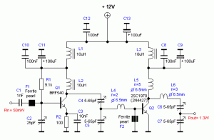
RF Amplifier circuit with 2SC1970 2N4427

Image
RF power amplifier circuit of this work is based on the transistor 2SC1970 and 2N4427. The set output power of 88-108 MHz FM RF Amplifier With 2SC1970 is about 1.3W and the input driver is 30-50mW. RF driver amplifier circuit uses a 2N4427 and its power amplifier using a transistor 2SC1970. At the time of the amplifier circuit tuning FM 88-108 MHz RF Amplifier With 2SC1970 should use the power meter / watt meter or SWR or RF field can also use the meter. RF amplifier circuit can work from the frequency of 88-108 MHz. RF Amplifier Circuit of 88-108 MHz FM RF Amplifier With RF 2SC1970 can radiate far enough. At the time of tuning you should use a 50 Ohm dummy load. For the input signal should be installed to regulate the VR level so as not to over-modulation (30-50mW).

2 7V 6 8A Power Supply by 723 and 7812

Image
In this 2-7V power supply circuit, for our purpose, we chose IC 723 instead of a three pin voltage regulator for-why we find it protean and more advantageous in technical details. Notes:  Heatsinks of Tr2 and Tr3 transistors must be sufficiently large. To archive R4,R5 and R6 values, we used some suitable resistors in parallel. For R4 and R5 two parallel connected 0.3ohm/5W resistors for each are used. To take 6A output, we connected two 0.22ohm/5W resistors in parallel, and to take 8A output we connected three 0.33ohm/5W resistors in parallel instead of R6 resistor. If you change the marked component values properly you can get up to 14V output. For this situation you must disconnect R1,R2,C5,C6,C1,C2,D1,D2  components and connect the positive terminal of D3 directly to the rectified and stabilized supply. TIP142 is a darlington transistor so you can not change it with other normal transistors. For an example of the circuit operation; When a 0.68 ohm load was connected, we desire

2W PA246 amplifier circuit

Image
This amplifier output circuit having a fairly low at only 2W 8 ohm impedance. Minimum supply voltage is needed 4 volts and a maximum voltage 18V DC. Power amplifier circuit was very low compared with other PA IC series, an average of 30W and over. Part List : R1 =  750K R2 = 100K R3 = 1K R4 = 18K R5 = 330K R6 = 82K R7 = 10K C1 = 5uF C2 = 100uF C3 = 1000pF C4 = 1000uF C5 = 0.1uF C6 = 5uF U1 = PA246

Non Switching Current Drive Amplifiers

Non-Switching Amplifiers Most of the distortion in Class-B is crossover distortion, and results from gain changes in the output stage as the power devices turn on and off. Several researchers have attempted to avoid this by ensuring that each device is clamped to pass a certain minimum current at all times. This approach has certainly been exploited commercially, but few technical details have been published. It is not intuitively obvious (to me, anyway) that stopping the diminishing device current in its tracks will give less crossover distortion . Current-Drive Amplifiers Almost all power amplifiers aspire to be voltage sources of zero output impedance. This minimizes frequency-response variations caused by the peaks and dips of the impedance curve, and gives a universal amplifier that can drive any loudspeaker directly. The opposite approach is an amplifier with a suffi ciently high output impedance to act as a constant-current source. This eliminates some problems – such as rising

0 30 Volts 2 5A Variable Power Supply Circuit Diagram

Image
This is the Simple 0-30 Volts - 2-5A Variable Power Supply Circuit Diagram. This is a high quality power supply with a continuously variable stabilized output adjustable between 0 and 30VDC. the LM 723 is the heart of the power supply which drives the BD137 and then the 2N3055. The circuit provides short circuit protection. And has great stability at voltage changes. Drive the circuit with 24 Volts 3A from a transformer. the 2N3055 needs a good heat sink. 0-30 Volts - 2-5A Variable Power Supply Circuit Diagram :

Simple Solid State Relay Circuit Diagram

Image
This is the Simple Solid State Relay Circuit Diagram. A higher Iiue voltage can be used if the diode, varistor, ZVS, and power thyristor settings are at compatible levels. For applications beyond triac current ratings, antiparallel SCRs might be triggered by the ZVS network. Simple Solid State Relay Circuit Diagram

Msc patran download free

Image
Enter your email Letters are not case-sensitive Find my account Password Stay signed in Gaining Upr convenience, keep this checked. On shared devices, additional precautions are recommended. Learn more Forgot password? Sorry, Google doesn't recognize that email. Create an account using that address? Something went wrong. Check your connection and try again. Sign in with a different account Create account One Google Account for everything Google

Simple Programmable Power Supply using LM317 Circuit Diagram

Image
Build a Simple Programmable Power Supply using LM317 Circuit Diagram . This is the Programmable Power Supply using LM317 Circuit Diagram type of the circuit simple and useful, it is a programmable DC power supply using LM317 . This circuit can set the output voltage for transistors.  The operation is simple, the transistors (T1-T4 = 2N2222 or any NPN transistors) are connected to resistors R which will grounded to determine the output voltage when one of the points ABC and D receives voltage, it makes the T corresponding drive your R to ground, so the voltage Vout changes according to the R, as you can see in the table below. The maximum voltage of this circuit is 27V when the input voltage is 28V.  Programmable Power Supply using LM317 Circuit Diagram This is when the output voltage of the DA is connected to Vin. (Values ​​of the resistors R) R Vout 100 1.8 330 3.0 470 4.0 1K 7.3 2.2K 13,5 3.3K 18,0