Posts

Showing posts from April, 2017

FPF270X Over Current Protection

Image
Using the FPF270X adjustable over-current protection IC can be designed a very simple adjustable current-limiting electronic project .FPF270X provide full protection to systems and loads from excess current conditions.Minimum current limit is adjustable from 0.4A to 2.0A.The input voltage range is 2.8V to 36V. Loads can be activated or deactivated with a low-voltage logic compatible ON pin. Fault conditions can be monitored using the error flag pin and/or the power-good pin. All devices clamp the load current so that it cannot exceed an externally programmed current level. An over temperature feature provides further device protection in case of excessive levels of power dissipation. FPF2700 responds to an overload condition that lasts longer than a fixed blanking period by turning off the load, followed by a retry after the auto-restart time.The FPF270X has an adjustable 0.4A to 2.0A minimum current limit set through an external resistor, RSET, connected between ISET and GND.A 4.7 F t...

Build Your Own RC Tankbot

Image
Here’s a blog post that will show you the setup you’ll need to make your own do-it-yourself radio controlled (RC) tankbot from the ground up. This example uses a few kits from Solarbotics to build your own RC controller, communication link, and tankbot using minimal parts. We even managed to get 250 feet of range out of the deal! For this exploit we invite you to move over to the dark side, as the heart of the project isn’t Xbees but instead 2.4GHz IEEE 802.15.4 Radio Frequency Network modules from Synapse Wireless which are actually super simple to use and configure. This post will merely get you started with building a general RC platform, feel free to modify/hack the system to suite your own diabolical requirements.

Memory organization 8051

Image
Memory organization is depends on type of architecture used. There are two type of architectures are used in controller or processor generally : 1) Von Neumann architecture 2) Harvard architecture Von Neumann architecture The term Von Neumann architecture, also known as the Von Neumann model or the Princeton architecture. This  architecture consist of address memory and data memory on a single unit . 8085 is based on Von Neumann architecture. Harvard architecture Harvard architecture consist of program memory and data memory as separate unit. Thus for accessing Harvard architecture we need separate address bus, data bus and control bus.  8051  is based on Von Neumann architecture.  Hence 8051 consist of two separate memory units, program memory as well as data memory. Program memory organization : The program memory organization for 8051 family is as shown in fig. above. 8051 microcontroller has an on chip internal  program ROM  of 4K size and if ...

Gus Driver Boost

Image

Simple Amplifier Schematic

Image
This Circuit Use a IC BA515 for operation it. This is very simple Amplifier schematic , with only add 8 component , such as resistor and capacitor. Minimum voltage require 3 Volt , this also low voltage amplifier . And maximum voltage require 9 volt . Power output under 10 Watt with impedance 4 Ohm . This circuit is very suitable for small speakers . See schematic below : If the circuit above not working may cause as follows : - Check voltage on the circuit , wether or not the voltage. - Check wether the components are soldered onto PCB properly. - Check input and output   wether working or not. - Check input output cable , if there are disconnected , or a short circuit. Or input connected with ground.

How Regulator with 2 Photocoupler

Image
Working of Regulator with 2 Photocoupler that is : Photocoupler N901 - used as a coupling-off control on the regulator by mikrokontrol. Which is set high and low voltage B + (st-by at the B + voltage is low). Control of the pin-37 POWER mikrokontrol → V610 → VD913 V908 → N901. Photocoupler N903 - used to control on-off the regulator of X-ray circuit protector. X-ray protector circuit of flyback → VD451 → VD452 → SCR VS472. If the flyback voltage regulator over the job will automatically be turned off by N903 To disable the X-ray circuit protector, it can be temporarily removed photocoupler N903 first. In normal conditions the voltage at the transistor V474 should be zero. Regulator Schematics Trobelshuting there is no voltage for 5v st-by on the secondary : Disable by removing the first circuit protectors N903 Check the voltage of 300V Check all transistors Check the start voltage of 300V by R909 >> R906 to the base of transistor power regulator Check the feedbac...

Telephone Line Monitor Circuit

Image
Circuit Diagram  Description   If you feel that somebody is tampering with your telephone line you might find this little circuit useful. It detects if there is another telephone connected to the line, if there is a short or an open line. Sound and a flashing light will tell you which is the current situation. The speaker is practically cut out during a normal conversation thus preserving privacy, only the LED will flash occasionally. The circuit does not require any battery and takes the supply from the telephone line itself. The transistors used are wired in a reversed biased fashion thus behaving as oscillators. You might try the 2N2222A as an alternative (not tested). This monitor is, of course, suitable only for analogue lines. Watch the polarity of the input line: the circuit will not be damaged by a polarity reversal but it will not operate correctly.  Author : smartkit Source http://www.electronics-lab.com/

Simple 3 Transistor Amplifier

Image
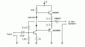
Mini 3 transistor amplifier is a simple amplifier with 50mW power drawn by 3 transitor. The series of three mini-amplifier transistors can be used for loud speaker 8 ohm load. Source voltage required to activate the mini-amplifier can be drawn from the batteries 9V.Rangkaian 3 transistor amplifier is often used in simple portabe audio devices such as radios or small tape recorder. Mini-transistor amplifier circuit 3 is quite simple as shown in the figure below. Mini-transistor amplifier circuit 3 includes type of amplifier OTL (Output Transformer Less). Mini-transistor amplifier circuit 3 is used for output coupling capacitors. Amplifier circuit is simple and suitable when used for audio amplifier experiment.

Telephone Line Powered LED Lamp

Image
This small and bright LED lamp is telephone line powered, means it uses the power of our telephone line. There are about -40v to -50v at telephone line, LM317T is used to adjust them according to our demand. 12 white LEDs of 5mm dia is used in this lamp, are all in series to compensate the voltage. Out of four wires of telephone only red and green is of our interest. This telephone line powered LED lamp is small, efficient and bright; one can also be use this for study or desk lamp. Schematic: Telephone Line Operated LED Lamp Components Required: BR2----------------------Bridge Rectifire U2------------------------LM617T or LM317L R3-------------------------270 ohm 1/2watt R4-------------------------6.8k ohm 12 white LEDs

Pulse Oximeter Circuit Diagram

Image
This circuit is a pulse oximeter , it is a medical device to indirectly measure the amount of oxygen in the blood of a person . The circuit is very simple and inexpensive to build , the sensor to be monitored only need an oscilloscope , but the case does not have an oscilloscope , here an article on how to make your pc a Oscilloscope . The operation is simple , light from an LED shines through on one side of your finger and is measured across the photo-transistor, a clothespin wood will engage the LED and the photo-transistor as a way to mount and align the sensor with finger . The monitor circuit uses only a single IC LM324 operational amplifier . There are three basic steps , the input signal is decoupled before being pre- amplified then passes through an adjustable low-pass filter to help eliminate noise 60Hz AC and finally a further low-pass filter in parallel with amplifier. Pulse Oximeter Circuit Diagram

Hofner Colorama II restoration project part 18 rescuing a ruined finish

Image
Well, it happens. You have a lovely finish on your guitar and then you drop it, chip it, scratch it, or whatever. In my case I got a bit overly energetic while polishing it and this happened: It probably didn’t help that the lacquer hadn’t completely cured so was still a little bit soft. I’m sure there’s a term for this, but I can’t for the life of me remember what it is. The long and sort of it is that I friction burned it, causing the lacquer to melt and shift. First things first, I decide to scrape off the raised lacquer with one of my favourite new tools, the razor blade: This leaves us with the following: Next, I carefully sand away any remaining effects left by the original melting using 400 grit paper wrapped around a wine bottle cork: This leaves us with this (you know that expression about things getting worse before they get better?) Next, we go over it with 600 grit paper, again wrapped around a cork (800 grit would be better if you can get your hands on some): Leaving us wi...

LED Driver for Automotive Applications using AT9933

Image
Using the AT9933 variable frequency PWM controller IC, can be designed a very simple and high efficiency LED lamp driver using a low-noise boost-buck topology.The AT9933 uses patent pending hysteretic current-mode control to regulate both the input and the output currents. This enables superior input surge immunity without the necessity for complex loop compensation. Input current control enables current limiting during startup, input under-voltage and output overload conditions. The AT9933 provides a low-frequency PWM dimming input that can accept an external control signal with a duty cycle of 0 - 100% and a high dimming ratio. This LED driver electronic project , require an input voltage range between 9 and 16 volts and will provide an 28 volt output at a maximum output current of 350 mA .The switching frequency of this electronic project is 350kHz . Values for components are : L1 = 82μH,L2 = 150μH,C1 = 0.22μF , RCS2 = 1.65Ω 1/4W, RREF2 = 10kΩ 1/8W, RS2A = 100Ω 1/8W,RS2B = 5.23kΩ 1/...

Simple Smoggy Schematic

Image
Even if your good old (Sony) Walkman  sees little use nowadays it would be a  shame to get rid of it altogether. The more  so when just removing the tape head  would allow the built-in audio amplifier  to become an outstanding electrosmog  detector for a variety of purposes. Looking at the schematic, readers with RF  experience will have no difficulty in recognising the diodes and coils of the two  detector-receivers, which serve to capture and demodulate RF signals. With its  coil of four turns (L2) one receiver covers the higher frequency range of the  electromagnetic waves, whilst the sec-ond detector takes care of the lower frequency range. Simple Smoggy Circuit diagram: For this reason a coil with a  greater number of turns is required: L1 is  an RF choke of about 250 µH. The precise  value is not critical and it could equally be  220 µH or 330 µH. The outputs of both detector-receivers  are connected to the...

Digital Electronic Lock Circuit Diagram

Image
This Digital Electronic Lock Circuit Diagram shown below uses 4 common logic ICs to allow controlling a relay by entering a 4 digit number on a keypad. The first 4 outputs from the CD4017 decade counter (pins 3,2,4,7) are gated together with 4 digits from a keypad so that as the keys are depressed in the correct order, the counter will advance. As each correct key is pressed, a low level appears at the output of the dual NAND gate producing a high level at the output of the 8 input NAND at pin 13. Digital Electronic Lock Circuit Diagram The momentary high level from pin 13 activates a one shot circuit which applies an approximate 80 millisecond positive going pulse to the clock line (pin 14) of the decade counter which advances it one count on the rising edge. A second monostable, one shot circuit is used to generate an approximate 40 millisecond positive going pulse which is applied to the common point of the keypad so that the appropriate NAND gate will see two logic high levels whe...

Small FAT Arduino Library SD Card Reader

Image
The library supports FAT16 formatted SD cards up to 2GB in size. 4GB FAT16 formatted SD cards might work, but is untested. Long file names are not supported. Keep you file names compliant with the old 8.3 standard. The SD card should be connected to the SPI-pins on your Arduino. Pin connections are available in the documentation in the download.

over under voltage relay operation

Image

Digital tone control with MAX5406

Image
The series will I make here is a series regulator of Volume, Bass, and Balance Trable Digital (Tone Control). The core of this circuit is an IC-type output from the Manufacturer Maxim MAX5406, while the IC is an audio processor that comes with the interface switch hit for Tone Control setting above. The circuit scheme is as follows: The scheme above uses very little supporting components and this makes can be made with a mini size of a matchbox only even if using all SMD components can be reduced in size by half for this time I will only give a simple layout made​​, following picture: layout components

10 000x With One Transistor Circuit Project

Image
For a collector follower with emitter resistor, you’ll often find that the gain per stage is no more than 10 to 50 times. The gain increases when the emitter resistor is omitted. Unfortunately, the distortion also increases. With a ubiquitous transistor such as the BC547B, the gain of the transistor is roughly equal to 40 times the collector current (Ic), provided the collector current is less than a few milliamps. This value is in theory equal to the expression q/KT, where q is the charge of the electron, K is Boltzmann’s constant and T is the temperature in Kelvin. For simplicity, and assuming room temperature, we round this value to 40. For a single stage amplifier circuit with grounded emitter it holds that the gain Uout /Uin (for AC voltage) is in theory equal to SRc. As we observed before, the slope S is about 40Ic. From this follows that the gain is approximately equal to 40I cRc. What does this mean? In the first instance this leads to a very practical rule of thumb: that gain ...

Schematic Audio Amplifier with IC TDA2004

Image
See this circuit below: Datasheet IC TDA2004 Vcc                = 8-18 V Pout               = 2X 12 W RL                  = 2 Ohm Ft                   = 20hz - 20Khz Icco                = 65 mA Package         = SIP1-11 Manufactered = SGS-ATES Other IC TDA2004 , In this circuit you can use the following IC : A2000V A2005V TDA2005 TDA2005M MPC2005 Or you can call Persamaan IC TDA2004

Build a 10W 225 400mhz Linear Amplifier Circuit Diagram

Image
Build a 10w 225-400mhz Linear Amplifier Circuit Diagram. This circuit broadband amplifier covers the 225-400 MHz military communications band producing 10 watt RF output power and operating from a 28 volt supply. The amplifier can be used as a driver for higher power devices such as 2N6439 and MRF327. The circuit is designed to be driven by a 50 ohm source and operate into a nominal 50 ohm load.   10W 225-400mhz Linear Amplifier Circuit Diagram   The input matching network consists of a section composed of C3, C4, Z2, C5 and C6. C2 is a dc blocking capacitor, and Tl is a 4:1 impedance ratio coaxial transformer. Z1 is a 50 ohm transmission line. A compensation network consisting of Rl, Cl, and LI is used to improve the input VSWR and flatten the gain response of the amplifier.  L2 and a small ferrite bead make up the base bias choke. The output network is made up of a microstrip L-section consisting of Z3 and C7, and a high pass section consisting of C8 and L3. C8 als...

Datasheet IC Amplifier AN7143 BA5406

Image
This time I will post about datasheet of some IC that was applied to the power amplifier. Some of his IC from IC AN7143, AN7145L, AN7145H, AN .... , Up to BA5406. Here is the datasheet it in the form of images that you can download. Datasheet IC Amplifier AN7143 - BA5406

3 A Wide input Adjustable Switching Regulator Project

Image
This is the simple project os 3-A Wide-input Adjustable Switching Regulator circuit diagram. The PTN78060 is a series of high-efficiency, buck-boost, integrated switching regulators (ISR) from good old Texas Instruments (TI). The caseless, double-sided package has excellent thermal characteristics, and is RoHs compliant. The PTN78060 devices operate from a remarkably wide input voltage range: Note that the –A version supplies a negative output voltage. The devices provide high-efficiency stepdown voltage conversion for loads of up to 3 A. The PTN78060 devices are suited to a wide variety of general-purpose applications that operate off 12-V, 24-V, or tightly regulated 28-V dc power, hence are ideal for running low-voltage electronics from a very high power 24-V battery unit salvaged from an electric wheel chair and migrated into a robot.  The output voltage VO can be set to any value over a wide adjustment range using a single external resistor RSET, using the equation RSET = 54....

NTSC PAL TV Signal Identifier Circuit Diagram

Image
This circuit is able to identify PAL and NTSC video signals. Its output is high for an NTSC signal and low if the signal is PAL. This output signal can be used, for example, to automatically switch in a colour subcarrier converter or some other device while an NTSC signal is being received. One application is for the reception from satellites of 'free-to-air' TV signals, which in Australia generally contain a mixture of 625-line PAL and 525-line NTSC programs. Operation of the circuit is as follows. IC1 is an LM1881 video sync separator which takes the video input signal and generates vertical synchronisation pulses. For an NTSC signal, these pulses are 16.66ms apart, corresponding to the 60Hz field rate, while for a PAL signal they are 20ms apart, corresponding to the 50Hz field rate. The vertical sync pulses are fed into IC2a, the first of two dual retriggerable monostable multivibrators in the 74HC123A. IC2a has a period of very close to 17.9ms, set by the 200kO resistor a...

Digital Clock with Timer and Solar Panel Regulator

Image
This is a combination digital clock timer and solar panel charge controller used to maintain a deep cycle battery from a solar panel. The timer output is used to control a 12 volt load for a 32 minute time interval each day. Start time is set using 9 dip switches and ends 32 minutes later. The 32 minute duration is set by selecting the 5th bit (2^5 = 32) of a 4040 binary counter (pin 2). The timer also has a manual toggle switch so the load can be manually switched on or off and automatically shuts off after 32 minutes. The time duration can be longer or shorter (8,16,32,64,128,256 minutes etc.) by selecting the appropriate bit of the counter. The timer circuit is shown in the lower schematic just above the regulator.   Basic Clock Circuit diagram The basic clock circuit (top schematic below) is similar to the binary clock (on another page) and uses 7 ICs to produce the 20 digital bits for 12 hour time, plus AM and PM. A standard watch crystal oscillator (32,768) is used as the tim...