Posts

Showing posts with the label circuit

DC to DC converter 1 5V to 3V Circuit Diagram
Image
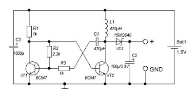
A DC-DC converter 1.5V to 3V Circuit Diagram to reduce the voltage is easy, but the situation becomes more complicated when we have to increase the voltage. This simple scheme generates a voltage 3Vdc from 1.5 VDC, which can be a single stack. We can get good results by modifying an multivibrator using two transistors, the frequency converter is approximately 130 kHz. The inductance value can be calculated experimentally. DC / DC converter 1.5V to 3V Circuit Diagram Schottky diode VD1 can be replaced by any other similar characteristics. For further stabilization of the output voltage can be placed one Zener 3V - 3.3V. This scheme can be used to feed a power LED device, a micro-controller, Arduino, etc. .. List of Components R1, R3: 1K R2: 2K2 C1: 470pF C2: 100uF / 3.3V C3: 1000uF L1: 470UH VD1: 15MQ040 VT1, VT2: BC547

24V to 12V 400W DC Inverter Circuit

Image
24V to 12V 400W DC Inverter Circuit Diagram 24V to 12V 20A 400W DC to DC Inverter. Does little to change my PV system 12v 24v me the problem arose of what to do with investors who already had 12V. I was looking for a pattern online and found several schemes with linear regulators 20A, this solution although quite simple, due to the huge losses they have is not advisable. Ideally, a converter switched, high-performance. At the end I found nothing I liked and decided to design my own. Circuit characteristics: Output current: 20A at 12V (15A continuous and 30A Momentary), Input voltage: 18 to 30V DC, Output voltage: 5 to 20V, Operating Frequency: 70kHz, Effectiveness: 95%, 400W maximum power, Protections: Above current (30A) in the F1 circuit, D1 and F1 polarity in the circuit.

Long duration timer circuit

Image
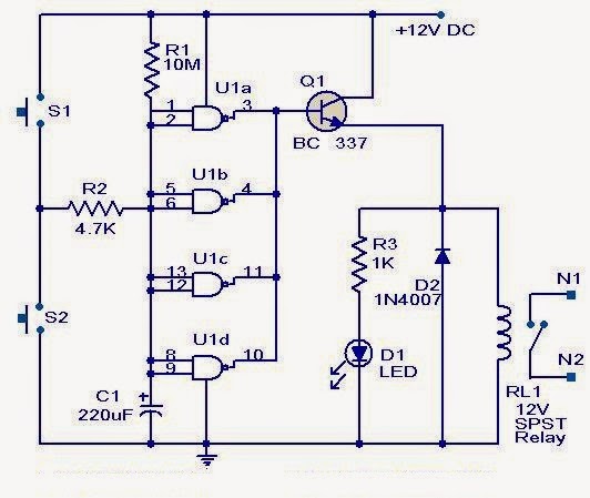
This timer circuit can be used to switch OFF a particular device after around 35 minutes. The circuit can be used to switch OFF devices like radio, TV, fan, pump etc after a preset time of 35 minutes. Such a circuit can surely save a lot of power. The circuit is based on quad 2 input CMOS IC 4011 (U1).The resistor R1 and capacitor C1 produces the required long time delay. When pushbutton switch S2 is pressed, capacitor C1 discharges and input of the four NAND gates are pulled to zero. The four shorted outputs of U1 go high and activate the transistor Q1 to drive the relay. The appliance connected via the relay is switched ON. When S2 is released the C1 starts charging and when the voltage at its positive pin becomes equal to ½ the supply voltage the outputs of U1 becomes zero and the transistor is switched OFF. This makes the relay deactivated and the appliance connected via the relay is turned OFF. The timer can be made to stop when required by pressing switch S1.

Motor driver L298 Circuit

Image
DC motor driver with H-Bridge IC L293D IC H Bridge DC motor driver L298 has two H-Bridge circuit in it, so it can be used to download the drive two DC motors. H Bridge DC motor driver L298 each can deliver currents up to 2A. However, in use, the H Bridge DC motor driver L298 can be used in parallel, so the ability to deliver the H Bridge DC motor driver L298 flow into 4A. The consequences of the installation of H Bridge L298 DC motor driver with the parallel mode, you need 2 pieces Bridge H L298 DC motor driver to control two DC motors using H bridge DC motor driver L298 in parallel mode. H Bridge Pin IC L298 DC motor driver which is connected in parallel operation mode: * OUT1 connected to OUT4. * OUT2 OUT3 linked. * IN1 is connected to IN4. * IN2 connected to IN3. * ENABLE ENABLE A linked to B. OUT1/OUT4 and OUT2/OUT3 associated with DC motors to be controlled. Please note that the output of the L298 does not have a safety diode. Thus, the need to add two diodes - flyback diodes, wit...

Glass Break Alarm Circuit Diagram

Image
This circuit can be used for sounding an alarm to detect the breaking of a glass window by an intruder, even when the intruder ensures there is no sound of the shattered glass. Fig. 1: Circuit of the glass break alarm Circuit and working    Fig. 1 shows the circuit diagram of the glass break alarm. It is built around a piezo element connected across connector CON2, transistor BC549 (T1), timer NE555 (IC1), a piezo buzzer (PZ1) and a few other components. A small piezo element used in the piezo buzzer is used as a sensor. It may be fixed at the centre of the window glass. IC1 is wired in monostable multivibrator mode, which is triggered by the piezo element. Output of IC1 is used to drive piezo buzzer PZ1. LED1 indicates the high-state output at pin 3 of IC1. Time delay can be adjusted by potentiometer VR1. Use an ordinary piezo buzzer at the output to generate a warning sound. This circuit works on 9V-12V DC. When an intruder tries to break the glass, the piezo element generat...

Smoke detector circuit

Image
This causes the resistance of LDR to increase and the voltage at the base of the transistor is pulled high due to which the supply to the COB (chip-on-board) is completed. The sensitivity of the smoke detector depends on the distance between bulb and LDR as well as setting of preset VR1. Thus by placing the bulb and the LDR at appropriate distances, one may vary preset VR1 to get optimum sensitivity. We have not build this smoke alarm detector. For smoke detector installation and maintenance use a near electrician.

Simple Transmission Indicator Circuit Diagram

Image
This is the Simple Transmission Indicator Circuit Diagram. This circuit the push-to-talk button is closed the light will go on. The antenna samples the output RF from the transmitter. That signal is then rectified (detected) by germanium diode Dl, and used to charge capacitor C2. Simple Transmission Indicator Circuit Diagram The dc output is used to trigger a small silicon-controlled rectifier (SCR1), which permits the current to flow through the small pilot lamp. For lower-power applications, such as CB radio, the antenna will have to be close-coupled to the antenna.

Over voltage Protection Circuit Diagram

Image
When testing a circuit, a source of voltage that is variable and has over voltage shutdown is veiy useful. In this circuit, Rl is adjusted to 1 to 2 V below the eventual shutdown threshold. R2 sets the trip voltage. When this voltage is reached, the circuit shuts the voltage to the circuit under test down. To reset, reduce Rl below trip threshold and depress reset switch SI. Over voltage Protection Circuit Diagram

One Condition Trimming Circuit Diagram

Image
One Condition Trimming Circuit Diagram . This relatively simple, inexpensive circuit requiring one trimming operation can multiply or divide with a consistent accuracy of greater than 1 part in 1,000. An inexpensive CMOS version of standard 555 timer chip T, in conjunction with low-drift LMll error amplifier A3, an inexpensive analog chopper switch SW, form a unique voltage-to-duty-cycle converter to produce the difficult transfer function necessary for accurate conversion. Read : Use 555 Build Spaceship Alarm  One Condition Trimming Circuit Diagram An unknown multiplicand voltage applied to the A3 error op amp circuit`s Y input controls the duty cycle of the timer through its pin 5 modulation input. The network between the sink-and-source output of the timer, pin 3, and the state trigger inputs, pins 2 and 6, cause the timer to oscillate. An error feedback signal from the timer`s discharge output, pin 7, represents the duty cycle. Integrating this duty-cycle signal with voltage re...

Voltage Regulator Circuit Using LM317

Image
The Voltage Regulator Circuit Using LM317 circuit diagram shows a way of powering a two-way mobile radio using the LM317T voltage regulator. The LM317 T is an adjustable 3-terminal positive voltage regulator that efficiently provides a load current of 1.5 Amps over an output range of 1.2 V and 37 V. With reference to the circuit, it can accept 14 volts without any hassle and the voltage can be controlled easily with the use of a potentiometer, a 3-terminal resister with sliding contact. The whole circuit will contain the following components: Printed Circuit Board (PCB) Resistor 1 (R1): 270 ohms Resistor 2 (R2): 2K carbon potentiometer Capacitor 1 (C1): 100nF Capacitor 2 (C2): 1uF tantalum LM317T Voltage Regulator Heat Sink DC Power Jacks Green LED: Power Red LED: Over Voltage Zener Diode: over voltage LED switch The zener diode switches on the over voltage LED if the voltage passing through is larger than the breakdown or preset voltage. The use of zener diode permits a constant amou...

Non Contact Power Monitor circuit Diagram

Image
Here is a simple non-contact AC power monitor for home appliances and laboratory equipment that should remain continuously switched-on. A fuse failure or power breakdown in the equipment going unnoticed may cause irreparable loss. The monitor sounds an alarm on detecting power failure to the equipment. The circuit is built around CMOS IC CD4011 utilising only a few components. NAND gates N1 and N2 of the IC are wired as an oscillator that drives a piezobuzzer directly. Resistors R2 and R3 and capacitor C2 are the oscillator components. The amplifier comprising transistors T1 and T2 disables the oscillator when mains power is available. In the standby mode, the base of T1 picks up 50Hz mains hum during the positive half cycles of AC and T1 conducts. Circuit diagram:     Non-Contact Power Monitor circuit diagram    This provides base current to T2 and it also conducts, pulling the collector to ground potential. As the collectors of T1 and T2 are connected to pin 2...

Pure Class A Headphone Amplifier Circuit Schematic

Image
Description  This design is derived from the Portable Headphone Amplifier featuring an NPN/PNP compound pair emitter follower output stage. An improved output driving capability is gained by making this a push-pull Class-A arrangement. Output power can reach 427mW RMS into a 32 Ohm load at a fixed standing current of 100mA. The single voltage gain stage allows the easy implementation of a shunt-feedback circuitry giving excellent frequency stability.  Tilt control:   The mentioned shunt-feedback configuration also allows the easy addition of frequency dependent networks in order to obtain an useful, unobtrusive, switchable Tilt control (optional). When SW1 is set in the first position a gentle, shelving bass lift and treble cut is obtained. The central position of SW1 allows a flat frequency response, whereas the third position of this switch enables a shelving treble lift and bass cut. Circuit Diagram:  Parts P1 = 22K Dual gang Log Potentiometer (ready for Stereo) R...

Radio Wave Alarm Circuit Diagram

Image
This simple circuit is sure to have the police beating a path to your door- however, it has the added advantage of alerting you to their presence even before their footsteps fall on the doormat. Simple Radio Wave Alarm Circuit Diagram : Notes : The circuit transmits on Medium Wave (this is the small problem with the police). IC1a, together with a sensor (try a 20cm x 20cm sheet of tin foil) oscillates at just over 1MHz. This is modulated by an audio frequency (a continuous beep) produced by IC1b. When a hand or a foot approaches the sensor, the frequency of the transmitter (IC1a) drops appreciably. Suppose now that the circuit transmits at 1MHz. Suppose also that your radio is tuned to a frequency just below this. The 1MHz transmission will therefore not be heard by the radio. But bring a hand or a foot near to the sensor, and the transmitter's frequency will drop, and a beep will be heard from the radio. Attach the antenna to a multiplug adapter that is plugged into the mains, a...

20 Watt Power Amplifier Circuit Diagram

Image
This IC chip was designed specifically for use in power boosting applications in automobiles. It is self protecting against short circuits and thermal problems. In the bridge configuration shown it will deliver 20 watts of power into a 2 ohm speaker operating at 14.4 volts. 20 Watt Power Amplifier Circuit Diagram

SIMPLE DOOR ALARM CIRCUIT

Image
SIMPLE DOOR ALARM CIRCUIT Here is the circuit diagram for simple door bell, you can assemble this circuit inside your room or home where as keep the switch outside your home or room that is easily noticable by the visitors. The working of this circuit is almost similar to my previous project. Simple Melody Maker Circuit Figure shows the circuit diagram of Simple door alarm.

Low voltage Power Supply Circuit Diagram

Image
If you want to check the behaviour of an electronic circuit at low voltages, an adjustable power supply as shown here may be helpful. Powered from a 3 to 16 volts source (DC for sure), it will provide a stable output voltage in the 0 to 1.5 V range. Adjustable Low-voltage Power Supply Circuit Diagram Multiturn trimpot P1 allows the output volt-age to be adjusted with good precision. The BC337-400 output transistor raises the out-put current to about 200 mA bearing in mind that the minimum supply voltage is 3.5 V. The transistor’s dissipation should be taken into account, and a more power ful t ype used if necessary. T1 may be omitted and R2 replaced with a wire link if you are happy with 3 mA at 3 volts out, 10 mA at 6 V or 20-30 mA at 10-16 V. These values represent the maximum output current of the TLC271 op amp. Without T1, the minimum supply voltage is 3.0 V. Author:Vladimir Mitrovic - Copyright: Elektor

Very simple stereo amplifier circuit with only need 4 components

Image
This is very very simple circuit audio amplifier  based on IC7057T  , you just use 3 components you can make this circuit . And the minimum voltage is 1 Volts , with just 1 Volt  you can operate this amplifier. Maximum voltage 6,5 volts . Maximum Power output 35mW with 32 ohms impedance. See circuit below : Very simple stereo amplifier

Emergency Siren Simulator Circuit Diagram

Image
This siren circuit simulates police, fire or other emergency sirens that produce an up and down wail. Simple Emergency Siren Simulator Circuit Diagram The heart of the circuit is the two transistor flasher with frequency modulation applied to the base of the first transistor. When the pushbutton is depressed, the frequency of oscillation climbs to a peak and when the button is released, the frequency descends due to the rising and falling voltage on the 22 uF capacitor. The rate of change is determined by the capacitor value and the 100k resistor from the pushbutton.  The oscillation eventually stops if the button is not depressed and the current consumption drops to a tiny level so no power switch is needed. The 0.1 uF determines the pitch of the siren: A 0.047uF will give a higher pitch siren and a 0.001 uF will give an ultrasonic (at least for me, anyway) siren from 15 to 30 kHz which might have an interesting effect on the neighborhood dogs! The 33k resistor from the collector ...

Connection Tester Circuit Diagram

Image
Description:    A low resistance ( 0.25 - 4 ohm) continuity tester for checking soldered joints and connections. Circuit diagram  Notes:   This simple circuit uses a 741 op-amp in differential mode as a continuity tester. The voltage difference between the non-inverting and inverting inputs is amplified by the full open loop gain of the op-amp. Ignore the 470k and the 10k control for the moment, and look at the input of the op-amp. If the resistors were perfectly matched, then the voltage difference would be zero and output zero. However the use of the 470k and 10k control allows a small potential difference to be applied across the op-amp inputs and upset the balance of the circuit. This is amplified causing the op-amp output to swing to full supply voltage and light the LED's.  Setting Up and Testing:   The probes should first be connected to a resistor of value between 0.22 ohm and 4ohm. The control is adjusted until the LED's just light with the resista...

TRAFFIC LIGHT CONTROL CIRCUIT USING NE555

Image